Intel Terminology
Intel has four "major processor families":
- Multiple super-fast processor chips used in super-computers, called the Xeon Phi family.
- Single very fast processor chips used in servers, called the Xeon family.
- Processor chips used in desktops, laptops, and notebooks, called the Core family.
- Very low power chips used in 5G communictions and the Internet of Things, called the Atom family (personal phones are excluded).
All Intel processors support the original x86 instruction set externally, but have very different micro-architectures internally. Some of the micro-architectures have evolved over time and are not the same as the original versions, but the family names have stuck.
Note: all processor "road maps" shown below are Intel generated.
Typical Product Numbering Scheme.
For example, lets look at an Intel Core i7-4700HQ chip.
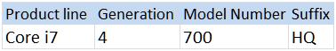
The above example is for the Core i7 product family, the top performance group of the Core products. "Core" chips come in three main versions i3, i5, and i7. This is the fourth generation of "Core" chips. The generation is the node (size of the transistor technology width) and micro-architecture designation. In the above case, it is the 22 nanometer (nm) production node with a fourth generation micro-architecture code named Haswell. Each generation of micro-architecture and node is given a code name. The exact model is the 700. The higher the number, the faster the processor. The HQ suffix designates the processor as a quad-core, meaning the chip contains 4 micro-processors. A "core" is one micro-processor. This exact numbering scheme is not used for other product families, but the Core family is the most popular one for business and residential customers. Other product family numbering schemes are similar but not exactly the same.
The Platform.
For example: The Basin Falls platform specifies the complete chipset architecture (X299) which includes the motherboard type, the socket type, the allowable processor chips, the memory types and memory access, bus speeds, overclocking, graphics support, etc. The Basin Falls specs (X299) can be seen here.
Revenue Reporting
Intel breaks down its revenue each quarter into several groupings as follows:
- CCG - Client Compting Group (revenue from desktop and laptop computer systems, Intel no longer supports tablets and phones).
- DCG - Data Center Group (revenue from cloud server chips, enterprise and super computer systems ).
- NSG - Non-Volatile Memory Solutions Group (NAND and 3D XPoint memory products).
- IoTG - Internet of Things Group and Mobileye (small electronic components and self driving car systems).
- PSG - Programmable Solutions Group (Altera acquisition - FPGA solutions).
- ISG - Intel Security Group (this group, formerly McAfee, no longer exists as it was sold in 2017).
The "Xeon Phi" Processors

In 2012, Intel announced that Xeon Phi would be the brand name used for products based on their Many Integrated Core (MIC) architecture. Xeon Phi chips are a family of chips delivering extremely high performance for workloads that are executed in parallel fashion. The first Xeon Phi product, code named Knights Corner, was announced in 2011, manufactured on a 22 nm (nanometer) process node (die shrink), delivered in 2012, and was in operational products in 2013. In Knights Corner systems, a Xeon processor (Ivy Bridge) was used as the main engine and the Xeon Phi chip, Knights Corner, was used as a co-processor. In the subsequent architecture, Knights Landing, the Xeon Phi chip can be used either as the main processor or as a co-processor. Knights Corner chips have in excess of 60 cores that can all be running at the same time. The Xeon Phi 7120 chip is capable of producing over 1.0 teraflops (TFLOPS - trillion floating point operations per second) of double precision floating point with 352 gigabytes per second (GB/sec) memory bandwidth.
By 2013 Xeon processors were ubiquitous in supercomputers - more than 80% of the top 500 machines in 2013 used them. For the very fastest machines, much of the performance comes from computer accelerators, i.e. the Xeon Phi. The first computers using Xeon Phi processors appeared in June 2012 and by June 2013 it was used in the fastest computer in the world.
A second generation Xeon Phi product, code named Knights Landing, on a 14 nm process was announced in June 2013 and shipments were made in late 2015 to early customers. See the Knights Landing chip package to the left. Note that the die size is extremely large. The "master die" is 3.5 inches wide by 2.25 inches high - much bigger than any previous full sized die. Note the "near" memory, called MCDRAM (multi-channel DRAM), composed of 8 small memory die of 2 gigabytes (GB) each located around the processor, making 16 GB total on the master die.
Intel says Knights Landing comes in two variants. The first will be a version mounted on an add-in board. In this case, Knights Landing plugs into a traditional server and acts as a co-processor. However, the other variant will come as a stand-alone processor. Intel is really playing up the stand-alone version and claims that more than 60 system providers will be selling units with Knights Landing as a stand-alone processor by the end of 2016. High performance computing (HPC) made up a significant portion of the company's data-center revenues in 2015 and it is expected to be a very fast-growing segment through 2018. See the Knights Landing Overview chart below.
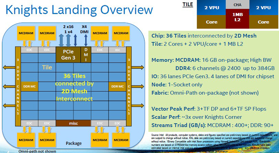
The cores on the Knights Landing chip are based on a heavily modified “Silvermont” Atom core that has four threads on it. (More on Atom chips below.) These are tiled in pairs, with each core having two AVX512 512-bit vector processing units (VPUs) and 1 MB of L2 memory shared across the tile. See the tile layout in the upper right hand corner of the chart. The tiles are linked to each other using a 2D mesh interconnect, which also hooks into the two DDR4 memory controllers that feed into the DDR4 "far memory". The far memory scales up to 384 GB capacity and delivers about 90 GB/sec of bandwidth on the STREAM Triad memory benchmark test. The 2D mesh also hooks the cores into eight chunks of high bandwidth stacked MCDRAM on-package memory, which scales to 16 GB of capacity. This is known as the “near memory” and offers more than 400 GB/sec of bandwidth to keep the cores well fed.
Intel has a number of different modes of memory addressing in the Knights Landing processor, including using the combined memory as a single address space or using the MCDRAM as an L3 cache for the DRAM memory. Add it all up, and Intel says that a Knights Landing processor delivers more than 6 teraflops of single precision and more than 3 teraflops of double precision floating point performance. Intel expects to ship more than 100,000 Xeon Phi units into the HPC market mainly in the second half of 2016.
See the four different versions of the Knights Landing chips below that Intel formally announced in June, 2016.
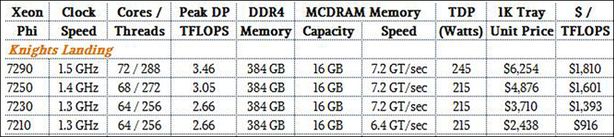
In the fourth quarter of 2016 Intel will ship the variants of these four Knights Landing parts with an on-package Omni-Path 100 series port. The Omni-Path Architecture (OPA) is a new high speed 100 Gb/sec (gigabits/sec. not gigabytes/sec.) Intel interconnect system to connect tens of thousands of nodes in an HPC environment. Adding the Omni-Path links to the chip package boosts the price by $278 and raises the thermal design point by another 15 watts. Two deals involving Omni-Path networking that have been publicly announced are at the Pittsburgh Supercomputing Center in the United States and Fudan University in China. Top
The "Xeon" Processors
Xeon Broadwell Processors - Version 4
The Xeon family of processors were traditionally aimed at the single socket server market. However, the newer E5 and E7 versions support multiple sockets. A processor "thread" is a sequence of active instructions in one core. A single-core computer processing unit (CPU) can have only one thread active at a time. A 2-core CPU has two threads active, one per core. Hyper threading is two virtual processors each sharing one physical core. Hyper threading can be utilized only with an operating system specifically optimized for it.
The Broadwell line (version 4) of very high performance processors are aimed towards the enterprise and workstation markets that are configured in single and two socket platforms. The Xeon E5-4600 v4 (4 socket platform) was announced in March, 2016. The Broadwell-EX/EN based Xeon E7-4800 v4 (4 socket platform) and Xeon E7-8800 (8 socket platform) were launched in June, 2016.
Broadwell-EP Xeon E5-2600 v4 processors feature up to 22 cores while the EX series will feature up to 24 cores. The 22 core version will feature a total of 44 threads and 48 for the EX. Intel has announced up to 55 MB of Level 3 cache on these processors. Maximum power ranges are from 145 watts to 165 watts.
The Broadwell Xeon E5-4600 v4 family is aimed at workloads that do not require the large memory footprint of the Xeon E7, which allows for up to 24 memory slots per socket compared to the 12 memory slots in the Xeon E5s. E5s are aimed at server vertualization and database acceleration, but not with the extreme memory capacity that is only available with the Xeon E7s.
The Xeon family of processors (as of June, 2016) is illustrated in the table below. Note the addition of three "Skylake" processors (version 5) in the E3 series in the table below. These were the first Xeon Skylake processors to be announced. The higher Xeon versions, E5 and E7, are still dominated by Broadwell (version 4) processors.
Intel Xeon Families (June 2016) |
|||||
Processor(s) |
E3-1200 v5 |
E3-1500 v5 |
E5-1600 v4 |
E7-4800 v4 |
E7-8800 v4 |
Core Family |
Skylake |
Skylake |
Broadwell |
Broadwell |
Broadwell |
Core Count |
2 to 4 |
2 to 4 |
4 to 22 |
8 to 16 |
4 to 24 |
DRAM Channels |
2 |
2 |
4 |
4 |
4 |
DRAM per CPU |
64 GB |
64 GB |
1536 GB |
3072 GB |
3072GB |
Multi-Socket Support |
No |
No |
2600: 1S or 2S |
Up to 4S |
Up to 8S |
PCIe Lanes |
16 |
16 |
40 |
32 |
32 |
Target Market |
Entry Workstation |
Memory Compute |
High-End Workstation |
Many-Core Server |
World Domination |
High End "Scalable Processor" (SP) Xeon Series Announced - Version 6
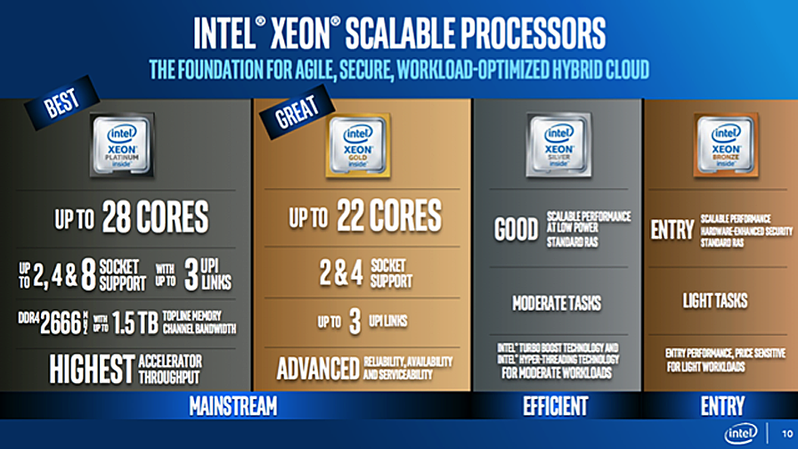
On July 11, 2017 Intel announced the latest generation of Xeon server processors based on the Skylake "Scalable-Processor" (SP) technology. The heart of Intel's new Xeon SP family, the "Purley" architecture, incorporates all of Intel's latest CPU and network technology and a large number of cores (28 in the top of the line processor). The SP product line comes in 4 versions: Platinum, Gold, Silver, and Bronze. (It is obvious that the old nomenclature of i3, i5, i7 and i9 has been discontinued in the server arena.)
Skylake SP offers five main benefits over the previous generation of Xeons:
- The high-end Skylake SP parts offer more cores topping out at 28.
- To better integrate all the cores and cache, they are now interconnected via a mesh rather than a ring topology.
- A 4 times larger 1 megabyte L2 cache (instead of a 256 kilobyte L2 cache).
- A new AVX-512, a 512-bit wide vector processor.
- The option of a direct Omnipath high-speed connection to/from the processor.
The new numbering system is quite complex, see Intel Xeon Scalable Processors for complete product details.
Google announced in February, 2017 that it would adopt the next generation of Intel Xeon processors for its data centers. Unbeknownst to almost everybody, Google was then already receiving shipments of Skylake SPs as the first customer. Intel disclosed in July, 2017 that it had already shipped about 500,000 SP processors to over 30 customers (with non-disclosure agreements). Based on testing by a number of cloud providers of early units, Intel is able to claim a substantial performance improvement - 1.65 average improvement over older Xeon processors.
In June 2017, AMD officially launched the EPYC line, their version of processors for data center servers. The EPYC top of the line has 32 cores and presumably more speed than Intel who has 28 cores. (However, real performance is based on more than simply core count (floating point throughput for example) so we will have to wait until some actual independent benchmarks are run to determine who is faster.) Cost is also a factor and AMD is the likely winner on price.
AMD did not announce a date for EPYC deliveries and most important, AMD did not announce a single data center win. The big question therefore: Is AMD actually getting significant orders for their new processors? Nothing is public on this yet and speculation is that actual orders are likely to be filled near the end of 2017. Even with faster processors, AMD may simply have arrived too late to win the battle for large data centers. However, they may be a very significant competitor for small and medium sized servers for data centers.
Intel Changes Its Processor Introduction Strategy
Historically, Intel's personal computer client chips, the Atom and Core families, got the first versions of any new processor technology (i.e. 14 nm Skylake) way before any of the Xeon families got it. In the case of Skylake, it took up to 2 years before the Xeon family introduced the new technology. The ramp up of a new process was perfected on client chips which have much higher volumes, and which allowed the production ramp to scale up faster than it would if it had debuted on server chips which have much lower volumes. In April of 2017, CEO Brian Krzanich said on a call with stock market analysts that the Data Center Group (Xeon family) would be a fast follower for the 10 nanometer process node and would come out ahead of the client chips on the 7 nanometer node. This was a major strategy shift.
Intel used the high volumes of the Client Group to drive down the costs of a new process. But, because of increasing demands for more compute power from high end Xeon customers and because of increasing competition from AMD and the ARM collective, Intel decided to revise its new chip introduction strategy. The Data Center computer chip price war will now be augmented with a process technology war. A technology war is one that Intel has demonstrated winning and can continue to win.
This move also has some economic impacts as some of the heavy startup costs of a new process technology will be shifted from the Client Group's P&L to the Data Center Group's P&L. However, it will not have any significant affect on Intel's P&L as a whole. Top
The "Core" Family Of Processors
Intel's "Core" brand of products are aimed at individual users ("Clients") and this product family makes up the bulk of computer processors on the market today. The current Core products come in five smaller groups: the i3,i5, i7, i7vPro, and the M series. Intel also offers Celeron and Pentium versions for entry level users at very good prices. Celeron versions are aimed at very budget oriented customers and have a very reduced version of the Core architecture. Pentiums are also based on a reduced Core architecture typically by lowering the clock frequency and disabling some features, such as hyper-threading, virtualization and some cache memory. (Current Pentium processors have only the name in common with the early Pentiums.) In general, the Core i3 is the everyday reasonably priced processor for the average user. It has good performance for the majority of people. The i5 is the medium processor for advanced scientific type users. The i7 is the top of the line processor for extremely heavy workloads (high-end gamers). The i7 vPro version has some features unique to advanced business users (heavy security and manageability). The M versions are the "mobile" equivalents of the desktop units and come in M3, M5, M7 and M7 vPro versions.
The chart below is an Intel originated chart showing the processor progression for mobile products from generation 6 (Skylake) to generation 7 (Kaby Lake) to generation 8 (Cannon Lake) to generation 9 (Coffee Lake) in early 2018. It is really hard for lay people to keep track of all the different processor versions in different market segments in shifting time frames. If all this sounds complicated, it is.
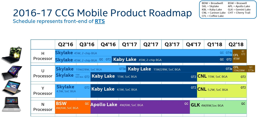
Lets look at the abbreviations at the left hand side of the above illustration.
-
The H processor line is the high end of the mobile CPU family such as gaming notebooks and very fast workstation laptops (45 watts).
-
The U processor line is meant for ultrabooks as well as portable 2-in-1s (15 watts).
-
The Y processor line is intended for low power processors in small portable units (4.5 watts).
-
The N processor line is for ultra low power entry level units such as IoT (Internet of Things) devices (4 watts).
What makes the generations different?
Gordon Moore, a co-founder of Intel, discovered that every two years the number of transistors in processors could be doubled. The cost of the wafers increased some, but the number of transistors double making the cost per transistor decrease dramatically. This became know as Moore's Law and has been good for 50 years. See the Moore's Law Section. Moore's Law is now universally used in the semiconductor industry to set future targets in research and development.
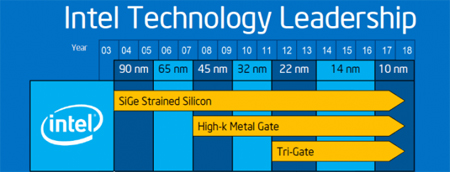
Intel and other chip suppliers now plan a new node (die shrink) every two years. See the technology chart to the left. A new node means that Intel can double the transistors on the same size die which then uses less power and generates less heat with an increase in performance. Between node advances every other year, a new more advanced micro-architecture is introduced. Hence there is a tick-tock rhythm to the semiconductor process. Every tick is a new node, every tock is a new advanced micro-architecture.
Ivy Bridge was a 22nm node ("tick") down from 32nm Sandy Bridge, while Haswell was a more advanced micro-architecture ("tock"). Broadwell was a new 14 nm node ("tick"), while Skylake is an advanced micro-architecture ("tock"). However, with Intel's announcement that Cannon Lake will be delayed about a year, Kaby Lake will be a second new micro-architecture from the same node. Intel now has a tick-tock-tock system in effect. The transfer from 14nm to 10nm is proving very difficult and we may be seeing 2.5 to 3.0 years between node upgrades in the future.
Core i3
Even though the Core i3 is at the base of the Core family, it is still a very good processor that has received very good reviews for its cost and performance by the majority of experts and customers alike. The technology behind Core i3 processors includes dual cores, hyper threading support, and virtualization. Core i3 processors also support 64-bit versions of Windows.
The important suffixes for desktop Core processors are K, R, and T. The K models have an unlocked core multiplier that makes them easier for enthusiasts to overclock the master clock (make it run faster). The R suffix is new for 4th generation parts and is used to designate a processor with Iris Pro integrated graphics. The T models are very low power versions built to draw as little power as possible. Standard laptop processors use the M suffix. New low-voltage parts meant for Ultrabooks and Tablets replace the M with a U or Y. Top
Core i5 and i7
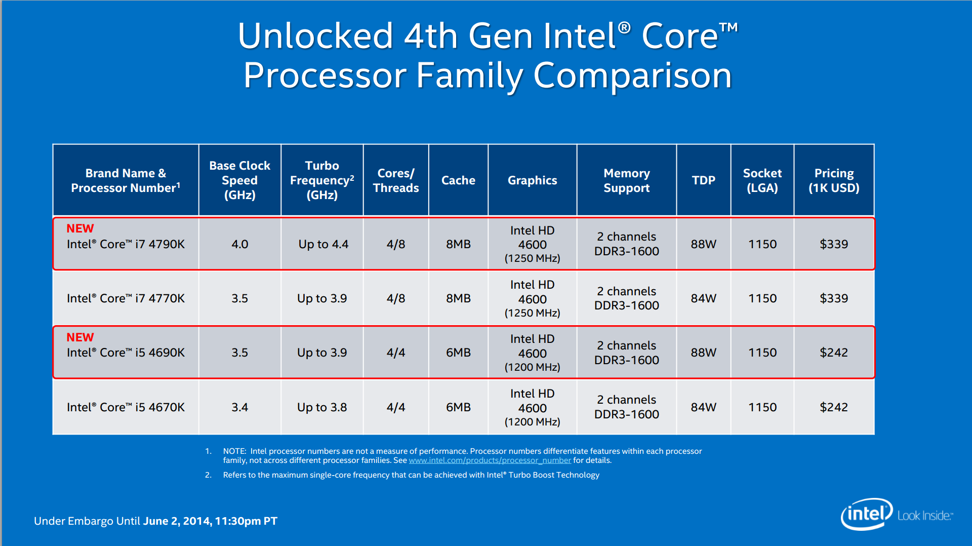
Core i5 and i7 processors are the “mid-range” and "high-end" processors produced by Intel. The above chart compares 4th generation (Haswell) i5 and i7 processors. Unlocked means that the base clock speed can be adjusted by the customer.
Note the base clock speed of 4.0 for the i7 (top line) is close to the maximum clock speed (maximum in a production computer environment is about 4.4 GHz as shown in the Turbo Frequency column). Note however, that the base clock speed is only a gross approximation of a processor's true speed.
The "micro-processor" clock speed can be as much as 10 times the base clock rate. Also complex instruction sets take longer to execute than do simpler instruction sets. Sometimes they are slower than simpler instructions, but sometimes faster depending upon the nature of the work involved. Benchmark runoffs are the ultimate test of a computer's speed.
Core i5’s offer enough performance to do video editing and gaming, and more than enough performance to do basic things like word processing, internet surfing, and email. A Core i5 processor is a great mid-range priced processor for people who use their computers frequently and multi task.
Core i7’s are the top of the line of Core series processors sold into highly technical environments and extreme gamers. They are also the most expensive. i7's have 4 more threads that can be running simultaneously and two more megabytes of cache memory than i5's. For most computer users, an i7 processor is not necessary. But... if you want the latest and the fastest, that’s what the i7 gives you. Top
Core M Processors
As mentioned above, the M processor series are mobile versions of the i3. i5, i7 and the i7 vPro. When talking about Core mobile processors we are discussing laptops and 2 in 1 type tablets, but not very small tablets, smart phones, or watches. When processors run they generate heat - lots of heat. Therefore the heat generated by the processor must be tightly controlled because of the space and cooling limitations in a thin portable computer.
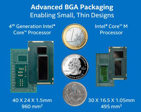
The 5th generation (Broadwell) Intel Core M processor package eats up just 495 square millimeters of space, about half the size of the 960 square-millimeter 4th generation package. See the illustration to the left. Note that the graphics processor and memory controller are integrated on the processor die.
In the i5 and i7 unlocked chart above for desktop processors, the heat limit is specified by the column TDP which stands for "Thermal Design Power", i.e. the amount of heat that the cooling system of the computer must dissipate. The i5's and i7's dissipate 84 to 88 watts of energy just from the processor chip. This is a fair amount of heat and heat sinks and fans are required to cool the processors. A similar TDP number for the Skylake (6th generation) mobile processors is 4.5 watts - a huge difference for very thin packages that operate without fans.
By in large, micro-architectures of the desktop and mobile processors of the same generation are similar. Programs written for a desktop will run unchanged on a laptop and vice versa. Portables do have a few different instructions that are unique to portables - such as powering down when the lid is closed. The main difference is in clock speeds. Laptop clock speeds are limited to 3 GHz or less. Cache sizes are limited to 4 megabytes versus up to 8 Mbs in desktops. Also, all Core M processors have 2 cores and 4 threads as opposed to 4 cores and up to 8 threads in desktops.
However, laptops provide very good overall performance, and in ordinary day to day workloads, perform as well as a desktop. Only special high performance workloads need to be done on a desktop these days. Top
Intel Announces Kaby Lake (7th Core Generation)
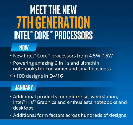
On August 30, 2016, Intel announced Kaby Lake - its 7th generation of Core processors. (Kaby rhymes with baby and is named after a lake in Canada.) As mentioned above, Intel has gone from a tick-tock series of architectures to a tick-tock-tock mode. Kaby Lake is the third set of 14 nm processors and the node (size of the transistor technology width) time has gone from 2 years to about 3 years between new node releases.
The move from Intel’s 14nm process to 10nm has been a long, slow one taking much longer than any previous new node introduction. The 14 nm process (Broadwell) was first introduced in Q3 of 2014.
The 10 nm processors (Cannon Lake) were initially expected to be produced in the second half of 2016. They were then delayed to the 2nd half of 2017, then the 2nd half of 2018, and finally to the 2nd half of 2019.
Intel no longer refers to the processor rhythm as tick-tock. It is now referred to as Process-Architecture-Optimization, or PAO for short. The first sector (Process) is a new manufacturing node, the second sector is a revised computer architecture, and the third sector is an optimized version of the architecture, called "14nm Plus" (14nm+ or recently 14nm ++) by Intel.
As can be seen from the Intel chart to the left, the various processor versions will come out in waves. The first wave will consist of three Kaby Lake parts of about 4.5 watts of power aimed at high-end tablets and 2-in-1 computers. Also, three more Kaby Lake parts at 15 watts will be dedicated to powerful notebooks (6 Kaby Lake models in all).
The fundamental micro-architecture between Skylake and the new Kaby Lake parts is practically unchanged. However, the "improved fin profile" (in the finFET transistor technology) is expected to produce a 12% to 19% CPU performance increase by running at higher clock frequencies with no increase in power. In addition, Kaby Lake has some nice upgrades of Generation 9 graphics aimed at the upcoming era of 4K ultrahigh definition (UHD) TV screen support (current TVs are 1K in number of screen pixels).
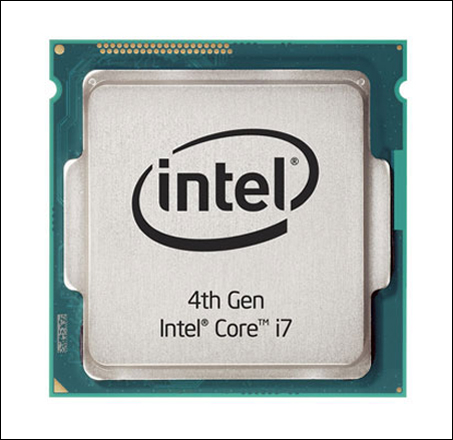
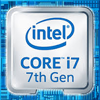
On January 3, at CES 2017, Intel announced the remaining line of Kaby Lake processors. Intel made a comprehensive update to its entire product line. See the Kaby Lake Core i7 processor pictured to the left. The initial Kaby Lake "mobile" refresh was limited to a handful of processors. With this launch Intel is bringing out a complete line of Kaby Lake processors intended for every price point. Kaby Lake is priced nearly identical to Skylake in almost every case.
Apart from the 4K ultrahigh definition (UHD) TV screen support, clock speed increases, and the Core i3-7350K (the first unlocked Core i3), the Kaby Lake family refresh is a pretty standard update to Intel’s road map. A little more clock speed, a little more performance, but not many new features to get excited about. However, to Intel's credit, squeezing an extra 8 to 10% performance out of Skylake with equivalent power is no small accomplishment given how hard it has been to move the ball on x86 performance. Top
Intel Announces The Core X Series Of Processors
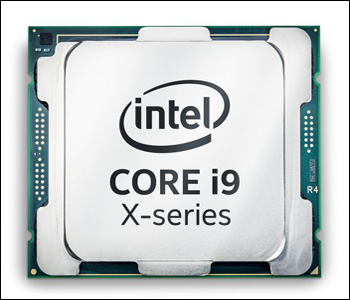
At the May, 2017 Computex Conference, Intel announced its new Core X family of processors aimed at the high-end desktop (HEDT) market. Intel is pitching this family of processors and the X299 chip set platform at gammers, content creators, and overclocking enthusiasts. The high-end desktop market is a relatively small one, but it's a market that's growing and a market in which customers are willing to pay a premium in exchange for higher performance.
The very top model - the Core i9-7980XE - packs 18 cores and carries a $1,999 price tag. Below that is the 16-core Core i9-7960X for $1,699, the 14-core Core i9-7940X for $1,399 and the 12-core Core i9-7920X for $1,199. The 10-core i9-7900X at $999 is much cheaper than the previous top of the line i7-6950X at $1650, making the 7900X a substantially better value than the 6950X. The prices for the lower core count (LCC = 10 or less) units are shown in the table below.
The new Core X lineup should invigorate enthusiasm in the gaming and PC enthusiast community for Intel's HEDT processors after the company seemed to neglect them for years.
The following five Core X processors will be available for shipment starting June 26, 2017.
Product |
i5-7640X |
i7-7740X |
i7-7800X |
i7-7820X |
i9-7900X |
Cores/threads |
4C/4T |
4C/8T |
6C/12T |
8C/16T |
10C/20T |
Base Clock |
4.0 GHz |
4.3 GHz |
3.5 GHz |
3.6 GHz |
3.3 GHz |
Turbo Clock |
4.2 GHz |
4.5 GHz |
4.0 GHz |
4.3 GHz |
4.3 GHz |
TurboMax Clock |
N/A |
N/A |
N/A |
4.5 GHz |
4.5 GHz |
L2 Cache |
256 KB per core |
1 MB per core |
|||
L3 Cache |
6 MB |
8 MB |
8.25 MB |
11 MB |
13.75 MB |
PCIe Lanes |
16 |
28 |
44 |
||
Memory Channels |
2 |
4 |
|||
Memory Type |
DDR4-2666 |
DDR4-2400 |
DDR4-2666 |
||
TDP |
112 W |
140 W |
|||
Price (1k tray) |
$242 |
$339 |
$389 |
$599 |
$999 |
The two 4 core processors above are Kaby Lake and the rest of the Core X line are Skylake processors. Intel plans to launch the 12-core Core i9-7920X gaming and PC processor on August 28, 2017 with the 14, 16, and 18 core models coming on September 25, 2017. The specifications for all the Core X models can be found here. Top
Intel Releases Its 8th Generation Of Core Processors
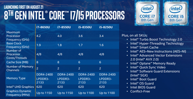
Intel's 8th Generation Core processors, code-named "Coffee Lake", were launched on August 21, 2017 (the same day as the total eclipse of the sun across the US). The first wave of 8th Gen U-series i5/i7 processors, meant for ultrabooks and portable 2-in-1s that consume only 15 watts, will ship to the market in September, 2017. But that’s just the beginning.
More 8th Gen Core 14 nm Coffee Lake processors will continue to roll out in the coming months. Desktop processors will start in the fall of 2017, followed by processors for enterprise customers.
Previously new Intel chips, whether they were die shrinks or new architectures, were assigned a new product number. With its 8th Gen chips, Intel is changing that policy. Unlike previous product generations, the 8th-generation family will span multiple chip families built on 14nm Plus (Kaby Lake), 14nm++ (Coffee Lake), and 10nm (Cannon Lake). Coffee Lake will pack up to six processor cores, rather than the maximum of four cores that the company has previously offered with this class of processors.
The above four U-series i5/i7 chips are fundamentally based on Kaby Lake with the same architecture and the same GPU (graphics processor). So what is new about these chips? Two things: they have larger core counts and slightly higher clock speeds. Intel expects a 40% overall performance improvement with the 8th Gen family versus the 7th Gen family. They expect 25% to come from the addition of two more cores with design and manufacturing improvements adding another 15%. This is all while improving energy efficiency resulting in a battery life of up to 10 hours.
However, according to outside experts, the 25% performance improvement due to the doubling of cores is lower than would normally be expected. This could be because Intel is either being conservative or because of power restrictions in keeping to 15 watts.
Ashraf Eassa of The Fool believes that the reason that Intel is keeping its high performance notebook and desktop processors on 14nm technology is cost. By late 2017/early 2018 Intel's 14nm technology will be quite mature while the company's 10nm technology will have just begun production and will be at the top of the product cost learning curve.
Also, a possible reason for moving the Coffee Lake chips forward to the fall of 2017 instead of early 2018 is because Intel wants to go head-to-head with AMD's Ryzen CPUs which were launched in March, 2017. The Ryzen chips are expected to give Intel a run for the money in both performance and cost. However, Intel will most likely hold its own in ultrabook class processors by using 4 cores whereas AMD uses only 2.
Intel Announces A Mobile "Core i9" Coffee Lake Chip And Other Mobile Processors
On April 3, 2018, Intel announced the Coffee Lake Core i9, which brings the firm’s most powerful CPU into the mobile space. The only Core i9 processor is the i9-8950HK, normally clocked at 2.9 GHz across its "six cores and 12 threads". The mobile i9 processor also has a massive 12 MB cache, and when unlocked for overclocking, can max out at 4.8 GHz.
Intel plans to continue its dominance of the mobile computing world with the release of the new Coffee Lake H-series processors (for high-end mobile laptops) and U-series processors (for ultrabooks) in addition to announcing Optane memory for the mobile market. All three of the new products are designed to give Intel what it needs to deliver top tier performance for every laptop price point and form factor.
Intel’s Coffee Lake U-series adds quad-core chips that range in clock speed from 2.3 GHz to 3.0 GHz with cache sizes from 4 MB to 8 MB. From Intel test data, a Core i5-8400U processor chip is 2.5x more responsive and 2.1x faster in office productivity tasks than a five year old similar system. The new U-series also integrates updated Iris graphics.
According to Intel, the new Optane mobile memory adds a 1.3x performance improvement in data writing and retrieval related tasks, in addition to a 4.7x improvement level when loading games.
Intel Announces Coffee Lake Entry Level Xeon Processors
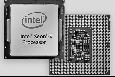
On July 12, 2018 Intel announced a series of entry level "Xeon E-2100 Coffee Lake" processors. While Xeon E chips are normally designed for workstations, they are also suitable for lower cost, single socket servers.
This family of processors have traditionally been used for entry servers for small and medium businesses and in more recent years positioned as edge computing engines. Also in the case of processors that have integrated graphics units activated, Xeon E can be used as video streaming units that have accelerated encoding and decoding. This class of chips has also found its way as X86 processors that are used inside of switches and as modest processors for cold storage arrays.
Historically we would have been expecting 10 nanometer Xeon E-class processors by now, but because of manufacturing and yield issues at Intel’s fabs, that is not hapening. Intel is relying on architectural tweaks, core, memory and peripheral expansions, plus pretty hefty price reductions on the Coffee Lake chips to give them a competitive option against low end AMD processors.
The big difference with Coffee Lake Xeon E-2100 chips is that the core count has been upped to six cores from 4, the L3 cache has been also increased to 12 MB, and the process tweak has allowed some of the Turbo Boost clock speeds to be jacked up by a few hundred megahertz. There are plenty of compute workloads in the datacenter and at the edge that could offload math to the floating point units on the CPU or GPU in a Coffee Lake chip, and do so at excellent price performance. Top
Intel Shows Off Cannon Lake PC
During Intel’s press conference at the CES 2017 convention in Las Vegas on January 3rd, 2017, CEO Brian Krzanich showcased a 2-in-1 PC sporting a processor based on the company’s “Cannon Lake” design. See the CES photo to the left. The chip was created using 10nm process technology, meaning Intel is able to cram even more transistors into a standard 12 inch wafer. Essentially, the lower the process number (10nm), the smaller the transistors are, creating more powerful, more power efficient chips.
For the last several years there has been a lot of talk about the death of Moore’s Law - that transistors will only get so small. However, Krzanich said that Moore’s Law is not dead and that Intel’s Cannon Lake processor design is a perfect example. “Moore’s Law is alive and well and flourishing,” he added.
Processors and products based on Intel’s Cannon Lake design are expected to ship before the end of 2017. Unfortunately, that is all Krzanich provided in regards to the embedded 10nm processor. However, he did indicate that 10nm process technology will help evolve the current virtual reality market thanks to slimmer devices, better power efficiency, and better computing performance.
Intel CEO Brian Krzanich Resigns
In June, 2018 Brian Krzanich was found to have violated company policy because of a past relationship with another employee. Intel found that Krzanich violated the company’s non-fraternization policy when he had a “past consensual relationship” with an employee of the company. The policy “applies to all managers,” the company said. Chief Financial Officer Bob Swan will serve as interim CEO. Swan has been with Intel since October 2016. Top
Intel Launches Whiskey Lake and Amber Lake Processors
In August, 2018 Intel formally announced six new processors for the Whiskey Lake U-series (15 watt processors for high power ultrabooks) and Amber Lake Y-series (5 watt maximum power processors for small portable units). There were three processors (i3, i5, i7) announced in each of the two families.
These new processors fall under Intel’s 8th Generation branding, which already contains Kaby Lake Refresh 15W processors. Per Intel, the reasoning for retaining the 8th Generation branding is that they consider the new parts to be very similar to those already out in the market (Kaby Lake) and contain only minor updates.
Intel's delayed 10nm process has held back the next generation Cannon Lake processors, so the company developed the 14nm++ Whiskey Lake and 14nm+ Amber Lake processors to fill the gap between generations and to give AMD some low end competition.
These new CPUs have modest improvements to their predecessors - tweaked maximum turbo clocks and a few chipset changes. Both Whiskey Lake and Amber Lake are Kaby Lake underneath, so there are no major micro-architecture or manufacturing changes.
In their 15 watt and 5 watt Core processors, Intel integrated the chipset into the same package as the CPU. This allows OEMs not only to save board space, but also increases the overall value of the processor and makes thermal management easier. The fact that Intel had not updated their Y-series CPUs since the original Kaby Lake launch in 2016 meant that the 5 watt notebook family were all overdue for an update. And even on the 15 watt U-series, there had been no improvements in the last year. So, these new announcements were critical from a competition point of view. Top
The "Atom" Family Of Processors
The "Atom" is the Intel brand name for its line of ultra-low-power processors. Atom processors are mainly used in netbooks, embedded applications ranging from health care to advanced robotics, and mobile internet devices (MIDs).
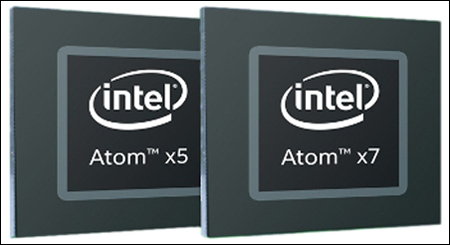
The Atom family of processors was first introduced in March of 2008. In December of 2012, Intel launched its first 64 bit versions of Atom processors. In March of 2015 Intel announced its x series of Atom processors which come in three versions: x3, x5, and x7 SoCs (systems-on-a-chip). The x5 and x7 (code named Cherry Trail) are 14nm technology.
The x3 chip (branded SoFIA) was aimed at computing devices priced under $75, while the x5 and x7 are aimed at products priced at $120 or more. The x3 also marks the first time Intel has been able to "integrate a modem" into a SoC, available in both 3G and LTE variants.
Intel Withdraws From Tablets And Phones
On April 26, 2016 Intel unexpectedly announced that it had made a major decision to drop the "mobile" versions of its Atom SoCs (Systems on a Chip), code named SoFIA and Broxton (smartphones and tablets), as part of their new revised strategy. Here is a summary paragraph of the strategic announcement of what is "in" at Intel by President Krzanich:
"Intel is accelerating its transformation from a PC company to one that powers the cloud and billions of smart, connected computing devices. We will intensify our investments to fuel the virtuous cycle of growth in the data center, IoT, memory and FPGA businesses, and to drive more profitable mobile and PC businesses. Intel delivers a broad range of computing and connectivity technologies that are foundational to this strategy and that position us well to lead the end-to-end transition to 5G. Our connectivity strategy includes increased investment in wired and wireless communications technology for connecting all things, devices and people to the cloud, and to power the communications infrastructure behind it. We re-evaluated projects to better align to this strategy."
What was "not included" in the strategic direction were "smartphones and tablets". Having fared poorly in mobile smartphones and tablets, Intel has abandoned its efforts to play catchup. It confirmed to trade publications that it was cancelling its Broxton and SoFIA chips designed for 3G and 4G phone technologies. Intel sent out a second message to trade publications clarifying that the Broxton Platform was being canceled for both smartphones and tablets, as tablets were not mentioned in the original message. Intel had invested billions of dollars subsidizing chip sales to tablet and low cost phone suppliers at huge profit losses to the company. However, Intel hasn't given up completely on smartphones as they have included the forthcoming 5G phone technologies in their strategic direction.
Also, Intel’s newest generation 14nm Atom platform, Goldmont, was announced at IDF Shenzhen in China in April of 2016 as part of the Apollo Lake netbook and low-cost PC platforms. So, it appears that Intel is not completely abandoning the Atom product family, just the current mobile smartphone and tablet "markets" that are not profitable for them. One other item not mentioned in the strategic direction is the future of the Intel contract semiconductor manufacturing business. It is currently not clear whether or not Intel is going to actively pursue its contract fab business.