Early Computer Memory
This web page is concerned with main computer memory, it does not cover hard drives or other auxiliary memory systems. Early computers used punched cards to both input the program and also to feed the program data. Punch cards were in common use until the early 1970s.
It should be noted that the use of punched cards predates computers. They were used as early as 1725 in the textile industry for controlling mechanical textile looms.
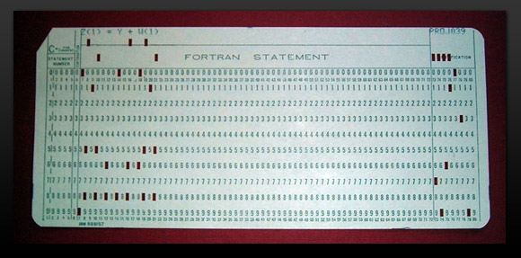
The card to the left is from an early Fortran program and says: Z(1) = Y + W(1). It was common in the early years for a Fortran program to be a card box or more in length. Input data might have taken many boxes. Program output could also be in punched card format or could be printed on a continuous ream of printer paper.
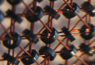
In he late 1940's Jay Forrester, a Professor at MIT, conceived the idea of a magnetic core memory with a grid of wires that could address each core. In 1951 he filed a comprehensive patent for matrix core memory. See the early enlarged photo to the left.
In 1953, MIT’s Whirlwind II Computer, became the first computer to use magnetic core memory. Whirlwind II was used for air defense command and control functions for the Air Force. The key breakthrough was the development of magnetic core memory that vastly improved the computer's reliability, operating speed doubled, and input speed quadrupled over the original Whirlwind I storage tube memory. It soon rendered all previous types of computer memory obsolete. Jay Forrester and MIT then licensed the core technology to IBM and other early computer manufacturers.
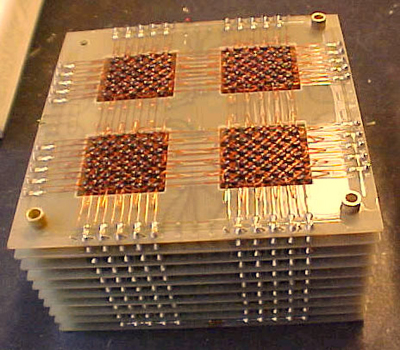
Core memory consisted of small rings capable of holding a magnetic charge. The wires could read or write bits by changing the magnetic direction. Each ring represented one bit. See the memory core rack to the left below.
Magnetic core memory was the predecessor to dynamic memory that we have today. It had a lifetime cycle of about twenty years, which was very long in those days of rapid change. Costs in the early days of core were upwards of a dollar a bit, but toward the end were under a penny a bit as manufacturing techniques got better and volumes increased dramatically. The cores got progressively smaller with each generation and were barely visible to the human eye at the end.
One interesting aspect of core memory is that the reading and writing of the magnetic fields actually imparts a small mechanical force to the cores. This mechanical force could cause a core to vibrate (ring) if the location in memory was repeatedly accessed at the right frequency. This caused problems with reliability in some machines, so much so that core memories were "potted" with a resin that kept the cores from vibrating.
However, a technology that involves a person handling each individual core during manufacturing can not compete with a technology that is basically a form of printing that lays down thousands of bits at a time. So, chip memory replaced core memory in the early 1970's. Top
RAM Memory Comes On The Scene
In 1966, Robert Dennard of the IBM Research Division, had the idea that binary information could be stored as a positive or negative charge on a capacitor. The only hitch was that capacitors leaked the charge off in milliseconds, so after several months of experimenting Dennard devised a configuration where a single transistor could read the charge and put it back thousands of times per second. A single transistor would be responsible for each bit of information. The constant refreshing of the charge on each capacitor is why Dennard's chip is referred to as "DRAM" (dynamic random access memory). Dennard was granted a patent for his field-effect transistor memory in June, 1968. However, IBM continued to use core memory in their computers for many more years.
In 1968 a new company, Intel, was started with a charter to design, manufacture and market semiconductor memory components. The company saw a huge market in the replacement of computer core memories by low cost memory chips produced in high volume.
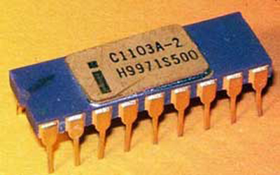
In 1969 Intel introduced the 1101, a 256-bit static RAM. However, the 1101 was too complex and had a small storage volume to achieve broad market acceptance. In the 1970 time frame, Intel was working on the 1102 and 1103, two different designs for a 1K (1,024 bit) dynamic RAM chip using three transistors per memory cell. For technical reasons, the 1102 never made it to the market.
With the introduction of the 1103 in 1971 (pictured above), the 1k dynamic RAM was a turning point in the history of integrated circuits. At first, production yields were poor and it wasn't until the fifth version of the pattern masks that it was widely commercially available. Now, a significant amount of information could be stored on a single chip which was price effective. It immediately began to replace core memories and soon became an industry standard. In 1972 it was the largest selling semiconductor in the world. Top
The Growth Of Memory Chips
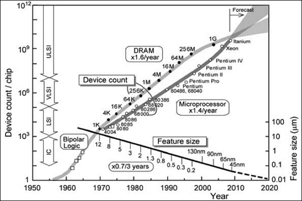
The chart to the left is quite busy, but focus on the upper curve which is the growth of memory chips over time. The Y axis is exponential according to Moore's Law. The x axis is time on a linear scale.
The Intel 1103 (from above) is labeled 1K in the year 1971. From there it is pretty much a straight line up to 256 Megabits in the year 1998. The 1 Gigabit level was reached in 2005 and one can see that the increase was beginning to slow down somewhat.
Forecasters predict that the increases will continue until at least 2025 but at a slower pace. History has shown that forecasting beyond 10 years is just guessing.
Not shown on the graph, is the latest chip from Samsung at 8 Gigabits (8Gb) announced in December of 2013, to ship in 2014. The chip is called the LPDDR4 Mobile DRAM. LPDDR4 is shorthand for Low Power Double Digit Rate 4. More about the exact meaning of this term below.
Samsung's technology for the chip was its leading edge 20 nanometer (nm) process technology. See the "Feature size" line on the bottom right of the chart above. It appears the "Feature size" projection continues to be a straight line per the forecast. Top
The Different Types Of Computer Based Memory
RAM (Random Access Memory) has become a generic term for any semiconductor memory that can be written to, as well as read from. All semiconductor memory, not just RAM, has the property of random access, which means that it takes the same amount of time to access any memory location. Therefore RAM data can be efficiently accessed in any random order.
This contrasts with other data storage media such as hard disks, which read and write data consecutively and therefore data can only be accessed in the same sequence it was written.
Volatile semiconductor memory loses its stored data when the power to the memory chip is turned off. However, it is usually faster and less expensive than non-volatile memory. Volatile memory is used for the main memory in most computers, since almost all data is stored on hard disks when the computer is turned off.
The major types of memory are:
-
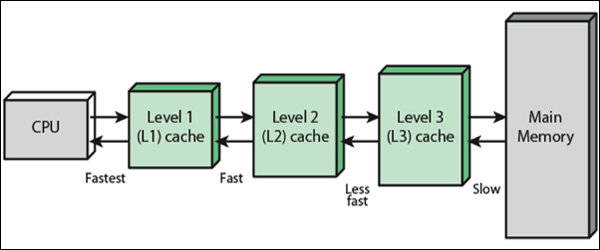
Cache Memory is used by the central processing unit (CPU) of a computer to reduce the time to access data from main memory. The cache memory is a much smaller, faster memory which stores copies of data from frequently used main memory locations. When the processor needs to read from a location in main memory, it first checks whether a copy of that data is in the cache. If so, the processor immediately reads it from its cache location which is much faster than reading it from main memory. The data cache is usually organized as a hierarchy of three cache levels - L1, L2, and L3. L1 being faster than L2, and L2 being faster than L3. See the memory illustration above.
-
SRAM (Static Random Access Memory) relies on several transistors forming a digital "one or zero" to store each bit. This is less dense and more expensive per bit than DRAM, but faster and does not require memory refresh. SRAM is used for the small cache memories in computer systems. However, SRAM is lost if the power goes down. While the power is on, it does nor need refreshing but it is still volatile.
-
DRAM (Dynamic Random Access Memory) consists of one capacitor and one transistor to store each bit. This is the cheapest and highest in density, so it had been used for the main memory in computers for years. However, the electric charge that stores the data in the memory cells slowly leaks off, so the memory cells must be refreshed (rewritten) many times a second. The refresh process is automatic and transparent to the user.
-
SDRAM (Synchronous DRAM) was a reorganization of the DRAM memory chip, which added a clock line to enable it to operate in synch with the computer's memory bus clock. The data on the chip is divided into "banks" so it can work on several memory accesses simultaneously in separate banks. It became the dominant type of computer memory by about the year 2000.
-
DDR SDRAM (Double Data Rate SDRAM) was an increased data rate enhancement, enabling chips to transfer twice the memory data (two consecutive words) on each clock cycle by "double pumping", transferring data on both the leading and trailing edges of the clock pulse. The SDRAM portion of the name is normally left off, but it really is SDRAM.
(Note: Extensions of this idea are the current techniques being used to increase memory access rate and bandwidth. Since it is difficult to further increase the internal clock speed of memory, DDR chips increase the data rate by transferring data in larger blocks.)
-
DDR2 transfers 4 consecutive words per internal clock cycle.
-
DDR3 transfers 8 consecutive words per internal clock cycle.
-
DDR4 transfers 16 consecutive words per internal clock cycle.
-
LPDDR 1-4 is "Low Power" DDR1 to DDR4 used in notebooks, tablets and high-end smart phones.
-
GDDR 1-5 (Graphics DDR1 to 5) GDDR5 has a 256 Gbit per second effective bandwidth per chip. GDDR chips are used for graphics cards, game consoles, and repeated high performance computations.
Intel & Micron Announce A New Memory Type
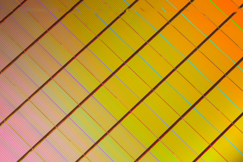
On July 27th, 2015, the IMFT joint venture partners, Intel and Micron, held a press conference and announced 3D XPoint (pronounced cross point) - a new class of memory. See the 3D XPoint wafer die to the left. It was the first new "mainstream" memory since NAND flash was announced in 1989. Intel and Micron claim they have been working on the new technology for about 10 years.
3D XPoint will be 10 times denser than DRAM, but not as dense as 3D NAND, 1000 times faster than NAND, but not as fast as DRAM. It will have 1000 times the endurance of NAND, but not infinite endurance. (Endurance is the total number of times a cell can be written or read.) Two very important features of 3D XPoint are that it is both Random Access Memory (RAM Byte addressable like DRAM), and Non-Volatile (NV) like NAND (does not lose information when power is turned off).
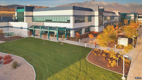
The new memory is also scalable. The first part out of the chute is 128 giga-bits (16 giga-bytes). (Two die shrinks and 3D XPoint begins to give 3D NAND competition.) The firms will provide sample wafers to customers by the end of 2015 and the chips will be in products shipping to customers in 2016. It will be manufactured at a fab in Lehi, Utah owned by the Intel/Micron joint venture. See the Lehi photo to the left.
There are other companies who have talked about new types of memory technology in the lab, but no one else is in mass manufacturing. 3D XPoint can be manufactured using current processes. There are some differences, but the partners claim the transition is akin to moving to a smaller die node.
So what makes this memory so unique and how does it work? First off, it does not contain any transistors, it is a resistive type of memory. Up until this point, all types of DRAM used transistors to indicate a one or zero. The partners have not at this time announced the exact materials that make up the storage cells.
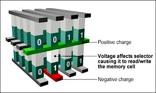
Each 3D XPoint die has 2 decks using 20nm technology. Perpendicular conductors connect 128 billion densely packed memory cells. Each memory cell stores a single bit of data. See the image to the left and note the green positive charge and red negative charge.
Each memory position has a "selector" shown in white in the image. The selector allows a specific memory cell (in dark green) to be read or written. The selector senses the voltage differential and enables a current to flow to the memory cell, which is either on or off. This compact structure results in very high performance and very high density.
Where does this technology fit in the memory hierarchy? A large memory gap exists between DRAM and NAND in terms of performance (speed), volatility (permanent or non-permanent), endurance and cost. 3D XPoint is aimed at filling this gap. Rather than copy data directly from slower types of storage into DRAM, software programs will anticipate what data is likely to be needed and then move it in advance to the 3D XPoint memory. Several analysts have speculated that in several years time, 3D XPoint will heavily impact the sales of DRAM memory. DRAM will be used strictly as a cache memory, while XPoint is used for main storage because of its lower cost, fairly high speed, and its non-volatility. We shall have to wait and see if this prediction plays out.
The Memory Wall
DDR4 and LPDDR4 are both just incremental improvements to a fairly old SDRAM basic design. Both standards improve power consumption and performance relative to DDR3/LPDDR3, but they are not a huge leap forward. Many of the underlying technologies baked into the standard were set a over a decade ago when total system bandwidth was a fraction of current levels and CPUs were all single-core. While there has been debate over whether or not to define a traditional DDR5, the industry consensus is that new solutions are now necessary. (However, some DDR5 may appear on the market.) Memory has become a major bottleneck with respect to performance and power goals. The performance limits imposed by traditional memory is referred to as the "memory wall". While the memory wall seemed insurmountable for a number of years, new 3D memory technologies are poised to tear down the wall. See the top contenders below. Top
Samsung "Wide I/O2"
The "Wide I/O2" specification, developed primarily by Samsung, is targeted for mobile devices. The original Wide I/O was not a success in the market because prospective users were looking for more performance and lower power than the original Wide I/O offered. Hence Wide I/O2 was born. Wide I/O2 defines a 3D memory stack and logical interface that is completely different than traditional LPDDR mobile memory.
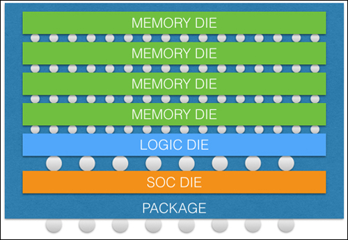
The stack is a 3D arrangement as shown in the illustration to the left. The memory die are stacked on top of the host chip, such as a system on a chip (SoC) die. It is a technology that is of most interest to companies building smartphones and tablets. These personal products have high resolution displays that put enormous pressure on their memory bandwidths while low power requirements are critical to their battery's life.
Performance is achieved by the use of Through Silicon Vias (TSVs) that greatly reduce the loading of the signal which improves both performance and power. The "wide" in Wide I/O comes from that fact that the bus width can be very wide, up to 512 bits. This optimizes the package’s size, but also imposes some thermal limitations because the heat radiated from the host die has to pass through the entire memory stack.
The wide bus with a lower transfer frequency (compared with LPDDR) delivers high performance along with lower power. The drawback to Wide I/O2, and all other 3D memory technologies, is cost. The precision alignment of the TSVs, additional manufacturing steps, and new handling procedures all contribute to higher cost. However, costs will be competitive after mass production which began in late 2015. Top
AMD High Bandwidth Memory (HBM)
High Bandwidth Memory (HBM) is a next-generation memory standard that will ultimately be used by most graphics processor units (GPUs) as the successor to GDDR5. The HBM specification is a standard managed by JEDEC, the Joint Electron Device Engineering Council that specializes in open standards for the microelectronics industry.
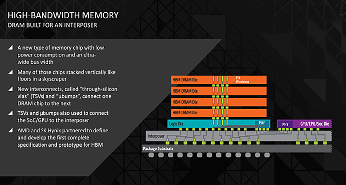
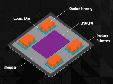
HBM is driven by AMD, Nvidia, and Hynix. This standard is targeted at high-performance graphics applications and networking applications needing ultimate performance. See the illustration above.
HBM has low power consumption, "ultra-wide communication" lanes and a new stacking configuration. HBM is an extension of the Wide I/O2 logic interface, but extends it to 4096 bits. Wow!
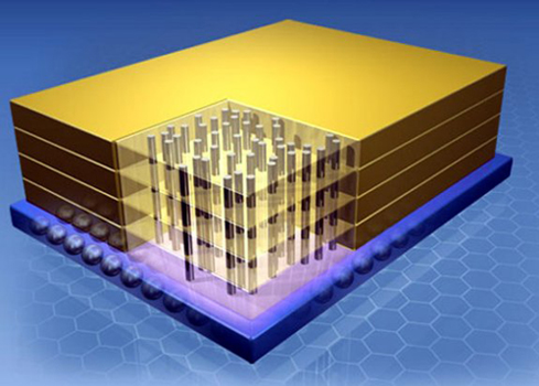
Also, the specification envisions up to 8 memory die stacked on top of each other and connected with TSVs. In HBM1, the stacks go up 4 dies high with the interface to each stack 1024 bits. The HBM processor arrangement consists of. a processor and 4 memory stacks on a large "interposer" chip.
The memory stack sits upon a logic die. The logic die may mount atop the target SoC chip or side-by-side on an "interposer" as shown in the illustration to the left.
The silicon "interposer" is a chip with just metal layers, no logic. The interposer is a very large chip whose purpose is to accommodate the ultra-wide 4096 bit memory bus between the CPU and the stacks.
HBM production is expected to ramp up in late 2015. More good info on HBM can be found here. Top
Micron Hybrid Memory Cube (HMC)
The Hybrid Memory Cube (HMC) is a joint development by Micron and Intel through their jointly owned IMFT partnership. The HMC standard is controlled by the Hybrid Memory Cube Consortium (HMCC) and is targeted towards very high speed server applications. The HMCC is backed by several major technology companies including Micron, Samsung, Altera, Xilinx, HP, ARM, and Microsoft. Memory manufacturers have to make their specifications public so that their computer customers can interface the products correctly. See the HMC illustration to the left.
Like Wide I/O2 and HBM, the HMC approach uses stacked 3D memory die connected by TSVs. Like the HBM memory above, the bottom layer is a logic die that handles the interface to the target chip. In a "near memory" application, the HMC stack would be placed on a large die next to the microprocessor. "Far memory" applications using many HMC modules would be separate from the computer module. This approach provides flexibility in memory architecture.
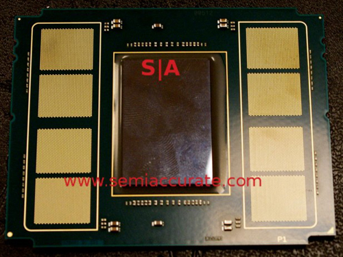
Pictured at the left is a "pre-release" picture of a new Intel Xeon Phi processor, code named "Knights Landing". The whole assembly is on one very big "master" die - a bit bigger than a credit card. The processor itself is in the middle. What is believed to be a hybrid of HMC "near" memory, composed of 8 die of 2 GB each, is located around the processor (16 GB total). This memory is called MCDRAM by Intel and has a proprietary interconnect between the processor and the MCDRAM memory.
The "master die" size has been estimated to be about 3.5 inches wide by about 2.25 inches high - much bigger than any previous full sized die. It was produced on a 14 nm process, also a market leader. Intel claims the data transfer rate is 5 times DDR4 (which is about 90 GB/sec of bandwidth). The 16 GB of "near" memory is the cache for 384 GB of "far" DDR4 memory (6 boards of 64 GB each).
Intel is expected to formally announce the Knights Landing system in the fall of 2015. (Speculation is at the SC 15 (Super Computer 15) event in Austin, Texas in November.) Xeon Phi processors are aimed at the extremely high performance parallel processing market of super computers.
It is well known that Micron shipped "second generation" samples of HMC memory in September of 2013. Micron's HMC is currently (mid 2015) believed to be in volume production and systems incorporating HMC are expected to ship in late 2015. The video on HMCC's Technology Page provides an excellent introduction to HMC technology. More info on Knights Landing processors can be found here. Top
How Do The Technologies Compare?
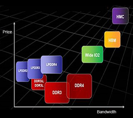
At the left is a chart developed by TSMC comparing the new memory technologies with existing ones. Although these new memory technologies are not in full volume production, TSMC, the world's second largest semiconductor manufacturing company behind Intel, is a very credible source for doing the comparisons.
Note that DDR4 memory is more expensive than DDR3 which indicates that the cost of DDR5 computer memory would probably be significantly higher with very little improvement in performance - hence the "memory wall".
Wide I/O2 is a significant bandwith improvement over LPDDR4 which it will replace in high performance tablets and smart phones at a modest cost increase.
HBM, led by AMD, is an enhancement to Wide IO2 and is a significant improvement in bandwidth but at a higher price. It is targeted at high performance graphics processors and network applications which are willing to pay a higher price for higher performance.
HMC, by Intel and Micron, is the highest in both performance and price. The first version of HMC is targeted for the supercomper market so it is not a surprise that it is the highest in price and performance. More info on the three different technologies can be found here.