Creating A Wafer
The semiconductor manufacturing process starts with making a wafer. Wafers are made of silicon extracted from sand. The main advantage of using silicon is that it is the second most abundant element in nature after oxygen. Sand has a high percentage of Silicon Dioxide (SiO2), which is the base ingredient for semiconductor manufacturing.
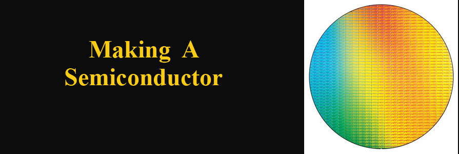
Once silicon is extracted from the sand, it needs to be purified before it can be used. Silicon crystals are produced by the Czochralski (pronounced Cho-crawl-ski) process, shown at the left, which was invented in 1916 by the Polish chemist Jan Czochralski.
Extremely high grade silicon, 99.9999999% pure, (one foreign atom per billion silicon atoms) is required for semiconductor applications. The process begins when the production chamber is heated to approximately 1500 degrees Celsius (°C) to melt raw silicon in a crucible.
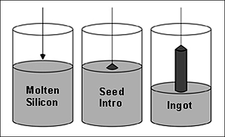
When the silicon is fully melted, a small precisely oriented seed crystal mounted on the end of a rotating shaft is slowly lowered until it just dips below the surface of the red hot molten silicon. The shaft rotates counter clockwise and the crucible rotates clockwise. The rotating rod is then drawn upwards very slowly, allowing an ingot to be formed. By precisely controlling the temperature gradient, rate of pulling, and speed of rotation, a large crystal cylindrical ingot is extracted from the melt. This is why finished wafers are all round discs. See the sample ingot to the left.
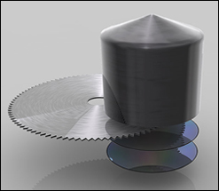
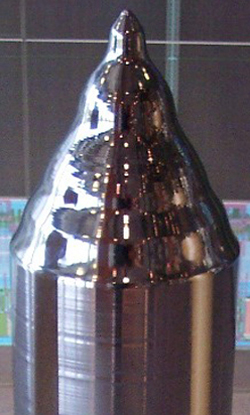
The ingot can be one to two meters in length depending on the amount of silicon in the crucible. This process is normally performed in an inert atmosphere, such as argon, and also in an inert chamber. Before it is completely cooled, the cone-shaped end of the ingot is cut off and the body is sliced into thin wafers of uniform thickness by a sharp diamond saw blade. See the slicing image to the right. (this and subsequent photos thanks to Intel.)
The cutting device is especially important in order to cut the ingot into very thin wafers 750 microns thick (0.03 inches thick). These thin wafers are brittle and very deliberate care is necessary in the handling of the wafers to prevent damage.
Wafers sizes have been growing over time as larger wafers yield more chips, higher productivity, and lower costs per chip. The most common wafer diameter used in semiconductor fabrication today is 300 millimeter (mm) or the somewhat older 200 mm wafer (12 or 8 inches in diameter). The first wafers in the 1970s were only 50 mm in diameter (2 inches). Top
Polishing And Oxidation
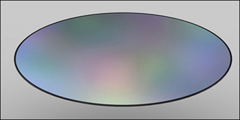
Sliced wafers need to be prepped before they are production ready. Machines polish the surface of the wafer into a mirror smooth finish. See the photo to the left of a super smooth wafer. A flawless super smooth surface allows circuit patterns to print better during subsequent processes.
The polished wafers start out in a pure non-conductive state. To make them semi-conductive, various substances are deposited onto the wafer and then specific circuit patterns are etched on the new surface.
Oxidation is a process in which a thin layer of silicon dioxide is deposited onto the silicon wafer. At very high temperatures (1000°C to 1200°C) oxygen is diffused into the wafer surface so that a thin smooth layer of silicon dioxide is created.
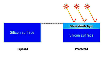
The silicon wafers are heated and exposed to ultra-pure oxygen in a diffusion furnace under carefully controlled conditions. When exposed to oxygen, an oxide layer begins to build on the wafer’s surface, just as iron rusts when it becomes oxidized in the air.
There are several oxidation methods, however thermal oxidation is most widely used. Thermal oxidation can be either wet or dry. Dry oxidation uses an atmosphere of oxygen to form a thin silicon dioxide layer. Whereas wet oxidation uses both oxygen and a vapor to produce a thicker layer. Although oxides created by the dry method have excellent electrical properties, they grow much slower than the wet method. Under identical time and temperature conditions, the wet method is five to ten times thicker than that of the dry method.
The silicon dioxide layer protects the surface from chemical impurities and pollutants that might penetrate during subsequent processing. Even tiny contaminants invisible to the naked eye can alter resistivity or conductivity and consequently damage the circuit’s electrical properties. Therefore, shielding the wafer surface with a protective layer is crucial. Top
Photoresist Coating And Patterning
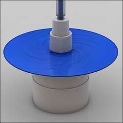
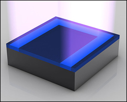
Photoresist is a light-sensitive liquid film that is applied to the wafer, giving it characteristics similar to photographic film. The photoresist liquid is poured onto the wafer as it spins at high speed. This spinning deposits a thin, even resist layer across the entire wafer surface. See the image to the left.
The photoresist can either be positive or negative depending on its reaction to light. Areas with positive photoresist are removed during the developing process when exposed to light, while those with negative photoresist remain.
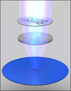
The photoresist finish is next exposed to ultra violet (UV) light, a process called photolithography or patterning. The chemical reaction triggered by this process is similar to what happens to camera film when the shutter button is pressed.
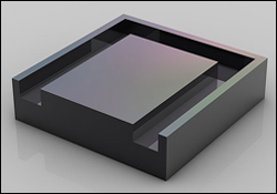
The "pattern" to be printed is formed on a mask that acts like a stencil. See the illustration to the right. When exposed to UV light, masks create the various circuit patterns for each layer of the chip. A middle lens reduces the mask’s image so the printed image on the wafer is typically four times smaller than the pattern of the mask. Everywhere the UV light strikes the resist, a chemical reaction takes place making those portions soluble. A stepper then systematically moves the pattern very precisely across the balance of the wafer completely covering it with the intended pattern.
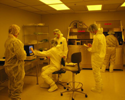
Pictured at the left is a cleanroom used in photolithography. A cleanroom is an environment, typically in chip research or manufacturing, with an extremely low level of environmental pollutants such as dust, airborne microbes, aerosol particles and chemical vapors. More accurately, a cleanroom has a "controlled" level of contamination. For example, a class 1 cleanroom allows only 12 particles of 0.3 μm and smaller per cubic meter. Wow! The yellow lighting is necessary in photolithography to prevent unwanted exposure of photoresist from random light of short wavelengths (no ultraviolet or blue light allowed). Top
Etching A Transistor
Although usually hundreds of microprocessors are built on a single 300mm wafer, we will focus on a tiny small piece of a transistor. Intel researchers have developed transistors so tiny that about 30 million of them could fit on the head of a pin.
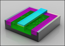
The soluble photoresist material (bright blue in the image to the left) is completely dissolved by a chemical solvent. This leaves the pattern in the photo resist made by the mask.
An etching chemical is then used to etch (dissolve away) the polished silicon dioxide material and a small quantity of the semiconductor substrate leaving a horseshoe shaped cut in the substrate.
Finally, the remainder of the photo resist material (dark blue in the image to the left) is removed through a another washing process, finalizing the cut in the surface of the wafer. See the small end product at the right. Top
Ion Implantation
The above process is repeated several times adding several layers to the transistor. Then it is time to do an ion implantation. In the ion implantation process (also called doping) the exposed areas of the silicon wafer are bombarded with specialty ions (usually atoms of boron or phosphorous).
These ions are implanted in the silicon wafer to alter the way the silicon in the particular area conducts electricity. Ions are shot towards the surface of the wafer and an electrical field accelerates them to a speed of about 185,000 miles per hour (300,000 km/h).
After the ion implantation, the photoresist (medium blue to the left) is removed and the green material that has been doped has specialty atoms implanted (to the right, the slight variation in the green color). Top
Copper Deposition
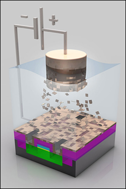
After a few more layers have been added, interconnecting copper wires are the next step. The wafers are put into a copper sulphate solution.
The copper ions are deposited onto the transistor through a process called copper deposition (or electroplating).
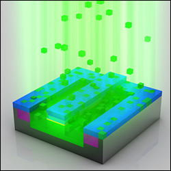
See the illustration to the left showing the copper ions floating down onto the top of the wafer. The copper ions travel from the positive terminal (anode) through the solution to the negative terminal (cathode) which is represented by the wafer.
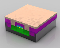
On the wafer surface, the copper ions settle as a thin layer of copper. See the illustration to the upper right.
The excess copper material is then polished off. See the final copper leads to the lower right.
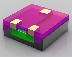
Current semiconductor fabrication includes several metal layers separated by dielectric layers. So the insulation layer operations and metal depositions will be repeated many times. A typical wafer undergoes hundreds of different operations and will take about a month to complete manufacturing. Top
Interconnecting Layers
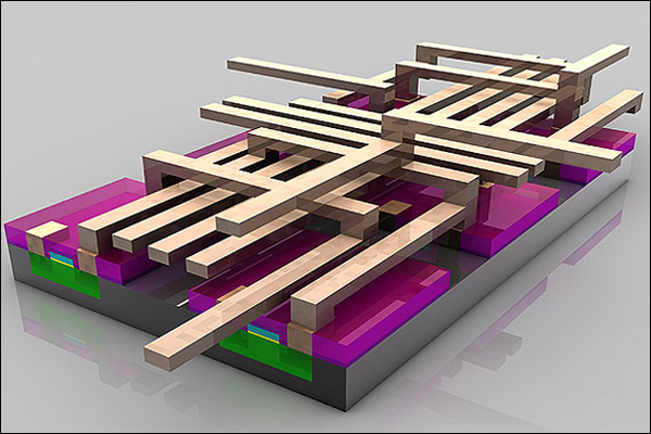
Multiple metal layers are necessary to interconnect the many transistors. How these connections have to be wired is determined by the computer's architecture and the specific design that the development team produced for a given processor.
While computer chips look very flat they may actually have 20 some total layers to accommodate extremely complex circuitry. They are comprised of a host of tiny copper bars that convey electricity from one tiny circuit to another.
A magnified view of a semiconductor chip is an intricate network of circuit lines and transistors that looks like a futuristic multi layered super highway.
Some of the circuits are directly connected, some are exactly a specific distance away from each other. All of them are used for one purpose: to move electrons in a particular way to in order to conduct “useful work” (such as adding two numbers together at very high speeds, the very essence of modern day computing). Top
Wafer Testing
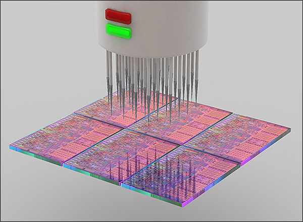
In the picture to the left, a section of the wafer is being put to a "first" functionality test. In this stage test patterns are fed into every single chip and the response from the chip is monitored and compared to an acceptable answer.
This level of testing includes not only traditional computational abilities, but also internal diagnostics, voltage readings, cascade sequences (does data flow through as it should), etc. And however a chip responds is stored in a database assigned to each die.
This process is repeated for every die on the wafer while all the dies are still on the surface. Chips that do not pass the test are marked with ink for rejection.
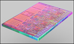
Next a tiny diamond-tipped saw is used to cut the silicon wafer into its numerous dies.
The database is used to determine which chips cut from the wafer are within specifications and kept, and which are discarded. Top
Core i7 Computer Die
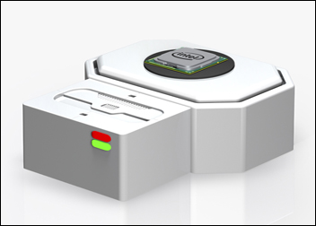
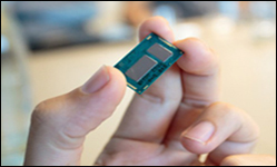
The final computer die, an Intel Core i7, is pictured at the left. The Core i7 die is assembled into a package that provides the contact leads for the chip. A wire-bonding machine attaches wires, a fraction of the width of a human hair, to the leads of the package. Encapsulated with a plastic coating for protection, the chip is tested one more time prior to delivery to the customer (see Binning below).
On the top of the chip package, a heat spreader is introduced. The metal heat spreader is a crucial component of modern high-speed semiconductors. In the past, a ceramic top was used with no active cooling. Modern computer chips generate enough heat to melt themselves in a few seconds. Only by having the heat spreader connected to a large heat sink can these chips operate long-term as they do.
Binning Operation
At this point the package is in its final stage. Still, there is one more step involved, called binning. In this process, the actual user characteristics of a particular chip are measured and recorded.
Items such as voltage, frequency, heat generation, compute performance, and characteristics of the cache, are all measured. The best chips are generally binned as higher-end parts, being sold as not only the fastest parts with their full caches enabled, but also as low-voltage and ultra low-voltage models.
Chips that do not perform as well as the best chips are sold at a lower price as slower clock speed models, or as a triple or dual core instead of their native quad core configuration.
Other chips may have some of their cache disabled which slows down their performance. Based on market demand, the highest-end chips can also be sold at lower-chip prices just to move them.
So, customers are offered a wide range of performance and prices for chips that all came out of the exact same wafer and all have an identical manufacturing history. Top
The Final Intel Core i7 Product
Pictured at the left, the final Intel Core i7 (14nm technology, code name Broadwell) was launched in Q1 of 2015. It has a 64 bit instruction set, 4 mega-bytes of cache memory, and a top speed of 3.1 gigahertz. It also has 2 cores (number of processors) and 4 threads (number of short sequences at one time, 2 per processor). For example, if one thread is waiting for data from memory, the CPU can process a second thread during the time it takes to fetch the original data from main memory or a hard drive. The Core i7 supports 16 giga-bytes of main memory and contains an upgraded graphics processor. The small chip at the top of the package is a platform controller hub (PCH) that optimizes input/output to/from the main computer chip. A super amount of compute power from a very tiny chip set!